Media Summary: Multidisciplinary product creation powered by your unconstrained network. Work concurrently across PCB In this video, we look at how to create a In this comprehensive video, Peter from Tech Explorations takes you through the entire process of
Designing A 4 Layer Pcb - Detailed Analysis & Overview
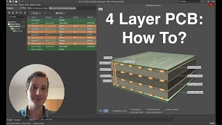
Multidisciplinary product creation powered by your unconstrained network. Work concurrently across PCB In this video, we look at how to create a In this comprehensive video, Peter from Tech Explorations takes you through the entire process of In this video I show you how to define your This video explains the basics of 4 layer PCB design using Altium Designer. You will learn how a typical 4-layer stackup is ... Thanks PCBWay for sponsoring this video - - Use this link for $5 new user free credit. Complete ...


![[PCB] PCB 4Layer Process](https://i.ytimg.com/vi/k6FrjFwjsds/mqdefault.jpg)


